Verilator Visual Simulator Architecture
Overview
When I was working on the FPGAScope project, I created this Verilator-based visual simulation tool to connect RTL hardware description with real-time interactive visualization. The system demonstrates how modern HDL simulation can integrate with SDL2 graphics to create responsive, dual-display visual testbenches for complex digital designs. These include PS/2 keyboard interfaces, VGA display controllers, and inter-FPGA communication protocols. The architecture highlights the power of cycle-accurate simulation combined with immediate visual feedback, speeding up the hardware development cycle from weeks to hours.
I built this tool because traditional FPGA development requires long synthesis before you can see how your design behaves on real hardware. This simulator eliminates that bottleneck by running Verilog/SystemVerilog designs in a high-performance C++ environment, with visual output rendered at 60fps. This enables rapid prototyping, real-time debugging, and immediate design iteration that would be quite challenging (at least for me!) with regular FPGA toolchains. See below for some of the examples discussed later.
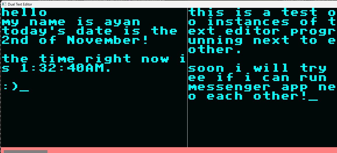
Early Development in FPGAScope Prototyping
The images above show the initial development of my FPGAScope project. It was much faster to visualize and
debug in software simulation than on hardware. The iteration speed is high because modifications to the VGA
controller, font rendering logic, or text buffer management can be tested within seconds rather than the
typical 20-minute FPGA compilation cycle. This was especially useful for the UI components which would
require calculation on where to place a given character in the charBuffer taking away
lots of time from other things.
The middle image above shows the initial proof-of-concept. Every clock cycle's VGA outputs (horizontal sync, vertical sync, RGB color values, and visible region flags) are captured and immediately rasterized to an SDL2 texture. Modifications to character ROM lookup tables, cursor positioning logic, or display refresh rates are instantly visible, creating a nice feedback loop that make it easy to experiment and refine.
Architectural Overview
The Verilator Simulation Engine
I chose Verilator because it's an open-source SystemVerilog and Verilog compiler that transforms HDL designs into optimized cycle-accurate C++ models. Unlike traditional event-driven simulators (ModelSim, Questa, DESim) that interpret RTL constructs at runtime, Verilator performs ahead-of-time compilation, generating native machine code that executes much faster faster than interpreted simulation. The compiled model exposes all module ports as C++ class members, enabling integration with testbench code written in C++. This makes Verilator ideal for the above given real-time visual simulation.
Verilator compiles the Verilog source into C++ source files organized into a class hierarchy where the top-level module becomes a C++ object with public member variables for each port signal.
// Example of typical Verilator API usage
#include "VtbDualMessengerVerilator.h"
#include "verilated.h"

VerilatedContext* contextp = new VerilatedContext;
VtbDualMessengerVerilator* top = new VtbDualMessengerVerilator{contextp};

// Initialize inputs
top->clock50MHz = 0;
top->resetn = 0;
top->scan_code_A = 0;
top->key_action_A = 0;

// Run simulation for one clock cycle
top->eval();  // Evaluate combinational logic
top->clock50MHz = 1;
top->eval();  // Rising edge trigger
top->clock50MHz = 0;
top->eval();  // Falling edge and settle

// Read outputs
uint8_t red_value = top->red_A;
bool vga_visible = top->visible_A;
System Architecture: Testbench, Hardware, and Visualization Layers
The simulation system is architected in three distinct layers, each with clearly defined responsibilities and interfaces. At the foundation lies the Hardware Layer, containing the actual Verilog RTL modules being simulated. This includes the text editor/messenger application logic, VGA driver modules that generate sync signals and pixel data, PS/2 driver modules that decode keyboard scan codes, and peripheral memory components like font ROMs and scancode lookup tables. These modules are written in synthesizable Verilog and are identical to what would be deployed on physical FPGA hardware, ensuring that simulation results accurately predict real-world behavior.
The middle Testbench Layer provides stimulus generation and signal routing between C++ and
Verilog. This layer is implemented as a special top-level Verilog module (e.g.,
tbDualMessengerVerilator) that instantiates the hardware modules and exposes control
and observation ports to Verilator. The testbench handles several responsibilities: it declares input
ports (clock50MHz, resetn, scan_code_A/B,
key_action_A/B) that accept stimulus from C++ code; it instantiates PS/2 keyboard simulator
modules (ps2KeyboardVerilator) that convert byte-level scan codes into realistic serial PS/2
clock and data waveforms; it connects communication signals between multiple board instances, emulating
inter-FPGA GPIO or serial links; and it exposes output observation ports (red_A,
green_A, blue_A, hSync_A, vSync_A,
visible_A, xOrd_A, yOrd_A) that allow C++ code to capture VGA signals
in real-time.
module tbDualMessengerVerilator(
    input clock50MHz,
    input resetn,
    input key_action_A,
    input [7:0] scan_code_A,
    input key_action_B,
    input [7:0] scan_code_B,

    // VGA outputs from board A
    output hSync_A, vSync_A,
    output [9:0] xOrd_A, yOrd_A,
    output visible_A,
    output [3:0] red_A, green_A, blue_A,

    // VGA outputs from board B
    output hSync_B, vSync_B,
    output [9:0] xOrd_B, yOrd_B,
    output visible_B,
    output [3:0] red_B, green_B, blue_B
);

    wire [7:0] commOut_A, commOut_B;
    wire commValid_A, commValid_B;

    // Cross-connect communication channels
    wire [7:0] commIn_A = commOut_B;
    wire commValidIn_A = commValid_B;
    wire [7:0] commIn_B = commOut_A;
    wire commValidIn_B = commValid_A;

    // Instantiate board A
    textMessenger boardA (
        .clock50MHz(clock50MHz),
        .resetn(resetn),
        .ps2Clk(ps2Clk_A),
        .ps2Dat(ps2Dat_A),
        .hSync(hSync_A),
        .vSync(vSync_A),
        /* ... VGA and comm ports ... */
    );

    // Instantiate board B
    textMessenger boardB (
        /* ... similar port connections ... */
    );

endmodule
The top Visualization Layer is implemented entirely in C++ and handles window management, user input, pixel capture, and frame rendering. This layer uses the SDL2 (Simple DirectMedia Layer) library to create cross-platform graphics windows with hardware-accelerated texture streaming. The core responsibilities include: SDL2 window and renderer initialization with specified resolution; event polling for keyboard presses/releases, mouse clicks, and window close events; scancode translation from SDL keycodes to PS/2 Set 2 scancodes with proper make/break sequences; simulation clock management running thousands of cycles per rendered frame to maintain real-time VGA timing at 50MHz simulation clock; pixel capture accumulating RGB values emitted by the Verilog VGA controller over the course of each frame; texture streaming uploading the captured framebuffer to GPU memory and blitting to the window at display refresh rate; and active board indication rendering visual overlays showing which virtual FPGA board is currently receiving keyboard input.
The main idea enabling this architecture is the separation of concerns between hardware and software. Verilog code remains pure synthesizable RTL with no awareness of the simulation environment; the testbench layer provides an interface between hardware and software; and C++ visualization code operates at the system level, managing clock generation, input devices, and output collection without modifying the hardware design with non-synthesizable constructs. This separation means the same Verilog modules can be simulated, synthesized to FPGA bitstreams, or even fabricated as ASICs without modification.
PS/2 Keyboard Interface Simulation
SDL Keycode to PS/2 Scancode Translation
The simulation layer must translate SDL keyboard events into authentic PS/2 scan code sequences. SDL
provides abstract keycodes (SDLK_a, SDLK_RETURN, etc.) that represent logical keys
independent of keyboard layout. I implemented a mapping table from SDL keycodes to PS/2 Set 2 scan
codes, which is the most commonly used PS/2 scan code set. Special keys have their own flags to handle the
their modification on a given scancode (i.e. capitalization using Shift)
space bar is 0x29,
Enter is 0x5A, Backspace is 0x66, and Tab is 0x0D. Shift keys have their own scan codes (left
shift is 0x12, right shift is 0x59), and we track them to handle make/break sequences.
uint8_t sdlKeyToScancode(SDL_Keycode key) {
    // Alphabetic keys (a-z)
    if (key >= SDLK_a && key <= SDLK_z) {
        uint8_t base[] = {
            0x1C, 0x32, 0x21, 0x23, 0x24, 0x2B, 0x34, 0x33,  // a-h
            0x43, 0x3B, 0x42, 0x4B, 0x3A, 0x31, 0x44, 0x4D,  // i-p
            0x15, 0x2D, 0x1B, 0x2C, 0x3C, 0x2A, 0x1D, 0x22,  // q-x
            0x35, 0x1A                                        // y-z
        };
        return base[key - SDLK_a];
    }

    // Numeric keys (0-9)
    if (key == SDLK_0) return 0x45;
    if (key == SDLK_1) return 0x16;
    if (key == SDLK_2) return 0x1E;
    // ... additional mappings ...

    // Special keys
    if (key == SDLK_SPACE) return 0x29;
    if (key == SDLK_RETURN) return 0x5A;
    if (key == SDLK_BACKSPACE) return 0x66;

    return 0;  // Unknown key
}
Make and Break Code Sequencing
Proper keyboard simulation requires generating make/break sequences with correct timing. When a user presses a key, the simulator immediately sends the corresponding scan code to the Verilog PS/2 keyboard module. When a user releases a key, the simulator must send a two-byte sequence, the first is the break code prefix 0xF0, then after a brief delay, the original scan code byte.
VGA Display Simulation and Pixel Capture
VGA Timing and Resolution
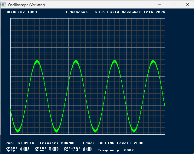
I configured the simulated VGA controller to operate at a resolution of 160x120 pixels with 4-bit color depth (16 colors), a deliberately low resolution chosen to maximize the simulation speed while remaining sufficient for text display and graphics. The simulator generates these signals at the same timing as would be required for real VGA hardware, ensuring that the synthesized FPGA Verilog will produce identical visual output.
Real-Time Pixel Capture
The C++ visualization layer captures VGA output on a pixel-by-pixel basis during simulation execution. On
each simulation clock cycle (after calling top->eval()), the testbench reads the exposed VGA
port signals from the Verilator model: visible_A indicates whether the current pixel is in the
active display region (not in blanking intervals), xOrd_A and yOrd_A provide the
current pixel coordinates as 10-bit values (supporting up to 1024x1024 resolution), and red_A,
green_A, blue_A provide 4-bit color components (values 0-15). When
visible_A is asserted and coordinates are within the valid 160x120 range, the pixel is
immediately stored in a framebuffer array.
I structured the framebuffer as a three-dimensional array
uint8_t pixelsA[VGA_HEIGHT][VGA_WIDTH][3], where the dimensions represent row index (Y
coordinate), column index (X coordinate), and color channel (R, G, B) respectively. The 4-bit hardware color
values are scaled to 8-bit RGB components using multiplication by 17 (i.e.,
red_8bit = red_4bit * 17), which maps 0→0, 15→255, and provides approximately linear
intermediate values. This scaling is necessary because SDL2 textures expect 24-bit RGB888 format (8 bits per
channel), and simply bit-shifting (e.g., red_4bit << 4) would produce only dark colors in the
upper half of the dynamic range. This actually was a problem as I had to debug why my colors were so dark
initially when I transferred the oscilloscope code to the real FPGA in the Lab.
// Pixel capture during simulation loop (called every cycle)
for (int i = 0; i < CYCLES_PER_CHUNK; i++) {
    top->clock50MHz = 0;
    main_time += 10;  // 20ns period = 10ns half-period
    top->eval();

    top->clock50MHz = 1;
    main_time += 10;
    top->eval();

    // Capture VGA pixels when visible
    if (top->visible_A && top->xOrd_A < VGA_WIDTH && top->yOrd_A < VGA_HEIGHT) {
        pixelsA[top->yOrd_A][top->xOrd_A][0] = top->red_A * 17;    // 4-bit to 8-bit
        pixelsA[top->yOrd_A][top->xOrd_A][1] = top->green_A * 17;
        pixelsA[top->yOrd_A][top->xOrd_A][2] = top->blue_A * 17;
    }
}
SDL2 Texture Streaming and Rendering
After accumulating a complete frame's worth of pixels (or the 60Hz timer is reached), the framebuffer is
uploaded to GPU memory via SDL2's
streaming texture API. The process begins with SDL_LockTexture(), which provides a writable
pointer to the texture's pixel data. The framebuffer is then copied row-by-row into the texture's memory
region. Each pixel's RGB components are
written sequentially as three bytes (R, G, B) in the texture's format.
For dual-board simulations, I doubled the texture dimensions horizontally (320x120 logical pixels), and the
left half receives board A's framebuffer while the right half receives board B's framebuffer. After
unlocking the texture with SDL_UnlockTexture(), the texture is rendered to the window using
SDL_RenderCopy() with a destination rectangle scaled by the SCALE factor
(typically 4x), transforming the 320x120 texture into a 1280x480 for easier viewing. A vertical
separator line is drawn between the two board views, and a colored indicator rectangle (green for board A,
blue for board B) shows which board currently receives keyboard input.
// Render frame (called after chunk simulation completes)
void* pixels;
int pitch;
SDL_LockTexture(texture, NULL, &pixels, &pitch);

// Copy board A (left half)
for (int y = 0; y < VGA_HEIGHT; y++) {
    for (int x = 0; x < VGA_WIDTH; x++) {
        uint8_t* dst = (uint8_t*)pixels + y * pitch + x * 3;
        dst[0] = pixelsA[y][x][0];  // Red
        dst[1] = pixelsA[y][x][1];  // Green
        dst[2] = pixelsA[y][x][2];  // Blue
    }
}

// Copy board B (right half)
for (int y = 0; y < VGA_HEIGHT; y++) {
    for (int x = 0; x < VGA_WIDTH; x++) {
        uint8_t* dst = (uint8_t*)pixels + y * pitch + (x + VGA_WIDTH) * 3;
        dst[0] = pixelsB[y][x][0];
        dst[1] = pixelsB[y][x][1];
        dst[2] = pixelsB[y][x][2];
    }
}

SDL_UnlockTexture(texture);

// Render to screen with scaling
SDL_RenderClear(renderer);
SDL_Rect dst = {0, 0, VGA_WIDTH * 2 * SCALE, VGA_HEIGHT * SCALE};
SDL_RenderCopy(renderer, texture, NULL, &dst);
SDL_RenderPresent(renderer);
Inter-FPGA Communication Simulation
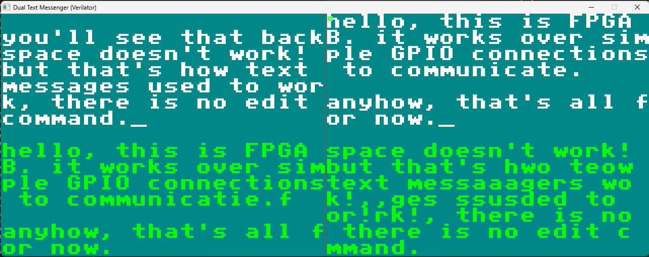
Dual-Board Text Messenger Architecture
The above shows a messenger test for allowing two boards to communicate, it gives us a simple way of testing
real-time bidirectional
communication between two simulated FPGA boards. Each board
runs an independent instance of the textMessenger module, complete with its own PS/2 keyboard
input, VGA display output, text buffer memory, and communication state machine. The system simulates a
realistic scenario where two physical FPGA development boards would be connected via GPIO pins, with each
board capable of sending 8-bit ASCII characters to its peer.
I kept the communication protocol basic to showcase the simulation tool rather than
implement complex networking stacks. Each board exposes four communication ports: commOut[7:0]
carries the 8-bit ASCII character being transmitted, commValid is a single-cycle strobe signal
indicating that commOut contains valid data, commIn[7:0] receives ASCII characters
from the peer board, and commValidIn indicates when incoming data is valid. The testbench
implements the physical wire connections by cross-coupling the ports: commOut_A → commIn_B,
commValid_A → commValidIn_B, commOut_B → commIn_A, and
commValid_B → commValidIn_A.
// Testbench wire cross-connection (in tbDualMessengerVerilator.v)
wire [7:0] commOut_A, commOut_B;
wire commValid_A, commValid_B;

// Cross-connect: A sends to B, B sends to A
wire [7:0] commIn_A = commOut_B;
wire commValidIn_A = commValid_B;
wire [7:0] commIn_B = commOut_A;
wire commValidIn_B = commValid_A;

textMessenger boardA (
    .clock50MHz(clock50MHz),
    .resetn(resetn),
    .commOut(commOut_A),
    .commValid(commValid_A),
    .commIn(commIn_A),
    .commValidIn(commValidIn_A),
    /* ... other ports ... */
);

textMessenger boardB (
    /* ... similar connection pattern ... */
);
Protocol Timing and Handshaking
The textMessenger module uses a valid-strobe (basically bit-blasting) protocol: the
sender places the ASCII
character on commOut and asserts commValid for one clock cycle. The receiver
samples on each rising edge and captures the data when commValidIn is asserted, writing it to
the receive buffer. This unidirectional protocol is lossy if the receiver isn't ready, but its design
makes it very easy for us to implement and test quickly.
I am sure that there are more advanced protocols out there, but this is a good starting point for at least getting this to work nicely. The plan here was to allow for two boards to communicate with each other in the raycasting setup below giving us multiplayer players moving on the same map together. I am told however trying to synchronize the clocks between the two FPGAs will require clock domain crossing.
The messenger simulation speeds up inter-FPGA communication development by skipping the synthesis-program-test cycle. On real hardware, each iteration takes quite a bit of time where you have to modify Verilog, synthesize and program both FPGAs, wire them up, run tests, analyze with oscilloscope, repeat. This is way better.
Build System and Compilation Process
Makefile Architecture
The build system runs through a very structured Makefile that manages Verilator compilation,
C++ compilation, and executable linking in a reproducible manner. The Makefile defines several
variables: VERILATOR_FLAGS specifies compilation options including --cc (generate
C++ code), --exe (create executable), --Mdir obj_dir (output directory), and
warning suppressions like -Wno-WIDTHTRUNC; VERILOG_SOURCES_MESSENGER lists all
Verilog files including RTL modules
(vgaDriver.v, ps2Driver.v, textMessenger.v) and testbench wrappers
(tbDualMessengerVerilator.v, ps2KeyboardVerilator.v); and LIBS and
LDFLAGS configure SDL2 linking with MinGW-specific static/dynamic library flags.
The compilation process works as follows:
- The
copy_mem_filestarget searches multiple possible locations forfont8x8.memandscancode.mem(font bitmap data and PS/2 scancode lookup tables) and copies them to the current directory, as Verilator's$readmemh()function expects memory initialization files in the working directory. - The
dualMessengerVerilatortarget invokes Verilator with all Verilog sources and the C++ testbench file (dualMessengerVerilator.cpp), specifying--top-module tbDualMessengerVerilatorto designate the testbench as the root of the module hierarchy. - Verilator generates C++ code in
obj_dir/and creates a makefile (VtbDualMessengerVerilator.mk). - The Makefile then appends SDL2 linking flags to the generated makefile by echoing
LIBS += $(LIBS)into the generated file, working around Verilator's lack of native SDL2 support. - Finally,
make -C obj_dir -f VtbDualMessengerVerilator.mkinvokes the generated makefile to compile the Verilator runtime library, generated C++ sources, and testbench C++ into a final executable.
# Verilator flags
VERILATOR_FLAGS = --cc --exe \
                  -Wall -Wno-fatal \
                  -Wno-WIDTHEXPAND -Wno-WIDTHTRUNC -Wno-UNUSEDSIGNAL \
                  --Mdir obj_dir \
                  -CFLAGS "$(CXXFLAGS)"

# Verilog source files for messenger
VERILOG_SOURCES_MESSENGER = \
    ../vgaDriver.v \
    ../ps2Driver.v \
    ../textMessenger.v \
    tb/ps2ClkDatVerilator.v \
    tb/ps2KeyboardVerilator.v \
    tb/tbDualMessengerVerilator.v

# Build messenger executable
dualMessengerVerilator: copy_mem_files $(VERILOG_SOURCES_MESSENGER) $(CPP_SOURCE_MESSENGER)
    $(VERILATOR) $(VERILATOR_FLAGS) \
        $(VERILOG_SOURCES_MESSENGER) \
        $(CPP_SOURCE_MESSENGER) \
        --top-module tbDualMessengerVerilator \
        -o dualMessengerVerilator
    @echo 'LIBS += $(LIBS)' >> obj_dir/VtbDualMessengerVerilator.mk
    @echo 'LDFLAGS += $(LDFLAGS)' >> obj_dir/VtbDualMessengerVerilator.mk
    $(MAKE) -C obj_dir -f VtbDualMessengerVerilator.mk
    cp obj_dir/dualMessengerVerilator.exe .
Optimization and Performance Considerations
The simulation for the messenger runs at roughly 2-5 MHz effective clock speed, meaning 50MHz hardware clock simulation executes in $50 / 2.5 \approx 20\times$ real-time. This slowdown factor is acceptable because human interaction (keyboard input, visual observation) operates at much slower timescales. I deliberately chunk cycle execution (simulating 8,333 cycles between frame renders) to maintain responsive 60fps display updates while maximizing throughput. This is similar to how FPS is maintained in the BareMetal Logic game when we take as much time to calculate TPS and then spend the rest of the cycle rendering to screen to maintain 60 FPS.
// Chunked simulation for responsiveness
const int CYCLES_PER_CHUNK = 8333;  // ~1/100th of a 60Hz frame

while (running) {
    SDL_PollEvent(&event);  // Handle user input

    for (int i = 0; i < CYCLES_PER_CHUNK; i++) {
        // Simulate one clock cycle
        top->clock50MHz = 0;
        top->eval();
        top->clock50MHz = 1;
        top->eval();

        // Capture VGA pixels inline
        if (top->visible_A && top->xOrd_A < VGA_WIDTH && top->yOrd_A < VGA_HEIGHT) {
            pixelsA[top->yOrd_A][top->xOrd_A][0] = top->red_A * 17;
            pixelsA[top->yOrd_A][top->xOrd_A][1] = top->green_A * 17;
            pixelsA[top->yOrd_A][top->xOrd_A][2] = top->blue_A * 17;
        }
    }

    // Render accumulated frame
    SDL_LockTexture(texture, NULL, &pixels, &pitch);
    /* ... copy framebuffer to texture ... */
    SDL_UnlockTexture(texture);
    SDL_RenderPresent(renderer);
}
(Ongoing) Raycasting Engine Development
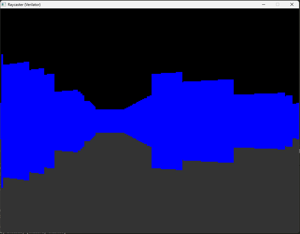
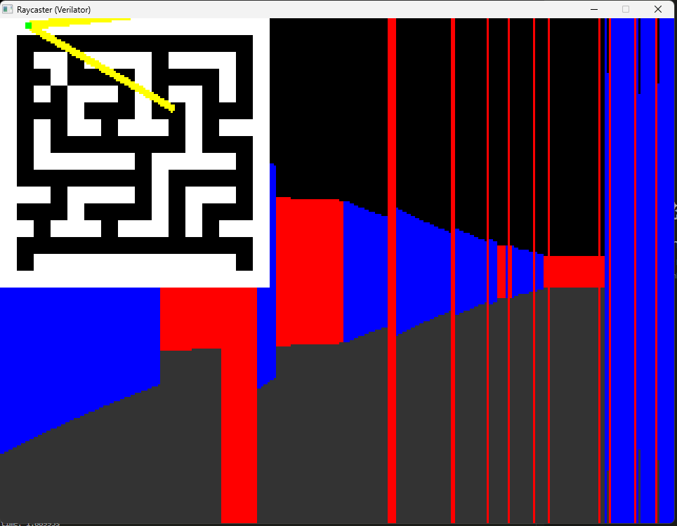
Rapid Prototyping of Complex Graphics Algorithms
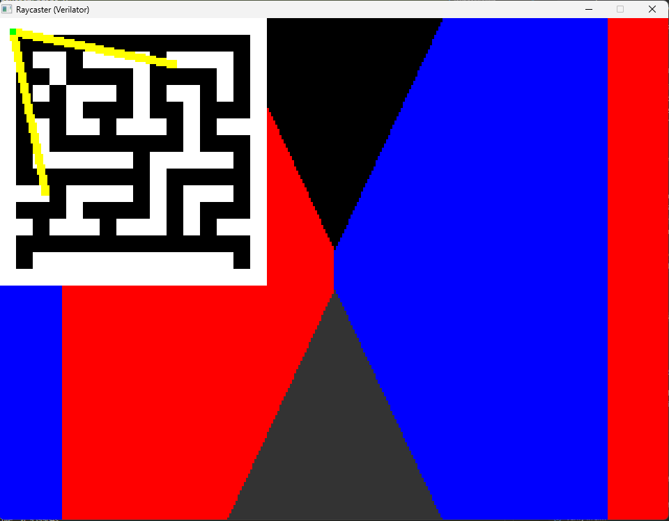
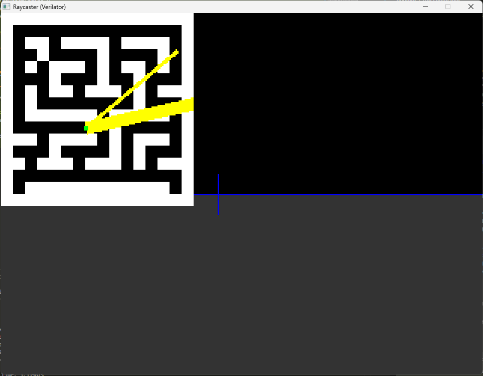
The above images shows the iterative development of a raycasting engine implemented in Verilog and simulated using this tool. Raycasting is a 2.5D rendering technique used in games like Wolfenstein 3D, where a 2D grid-based map is rendered with perspective projection by casting rays from the player's viewpoint to detect wall intersections. Implementing raycasting in hardware is non-trivial (at least for me!), requiring fixed-point arithmetic for fractional coordinates, trigonometric lookup tables for angle computations, and pipelining of the ray-marching algorithm (given that raycasting is a sequential ray-marching algorithm) to meet timing constraints. The images show off the development process, where initial attempts produce scrambled or empty output, suggesting fundamental issues with coordinate transformations or memory addressing; later there is partial rendering with visible artifacts like incorrect wall heights or coordinate system inversions; and below is an almost working version.
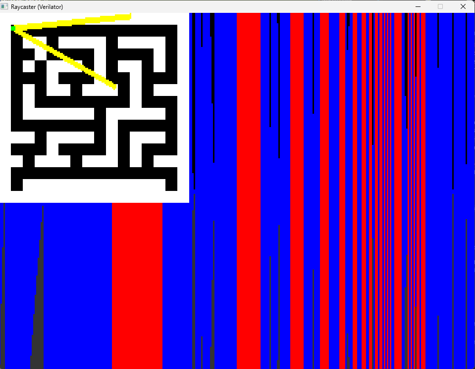
Final Working Implementation
The image above shows the end result of the development process, it has't yet been exactly working as expected but it gets quite close.
The raycasting engine uses a pipelined architecture where each clock cycle processes one pixel column.
- Computes the ray direction based on player angle and current column index using precomputed sine/cosine lookup tables.
- Performs DDA ray-marching through the 2D map grid using fixed-point increments.
- Detects wall intersections by checking map cells until a non-zero value is found.
- Calculates wall height using the formula $h = \frac{k \cdot f}{d}$ where $k$ is a scaling constant, $f$ is the focal length, and $d$ is the perpendicular distance to the wall.
- Outputs RGB color values with distance-based shading applied.
At 160 pixels horizontal resolution, the engine can achieve $\frac{50 \text{ MHz}}{160 \text{ pixels}} \approx 312 \text{ kHz}$ frame rate theoretically, though practical implementations are limited by VGA timing to 60Hz.
Future Developments
I would like to develop a tool that enables quick development of programs using high-level HDL languages like Silice while also writing C programs. This would allow developers to very quickly write highly performant programs for MCU-FPGA systems such as pairings like ATMegaX-IC40X, enabling highly performant, low power consumption systems where we can perfectly optimize for both performance and power efficiency. The platform would expose a unified toolchain for cross-compilation, cycle-accurate co-simulation, and easy packaging so prototypes can be verified and iterated quickly just like FPGAScope or the raycaster was.
A cool idea would be to have a very limited piece of hardware like that run a full game like Comanche: Maximum Overkill from 1992 on a power consumption of less than 1W (or that order of magnitude when comparing how much energy it took to run back in 1992).
The tool would allow someone to very quickly write in C (or C++), find the functions or algorithms that take the longest by some nice development environment that automatically places timers and then allows the user to implement the slow (or costly functions) in some high-level HDL like Silice (as we can get the biggest performance gain as it is the highest cost) and compile all in one integrated test environment just like I've done above.
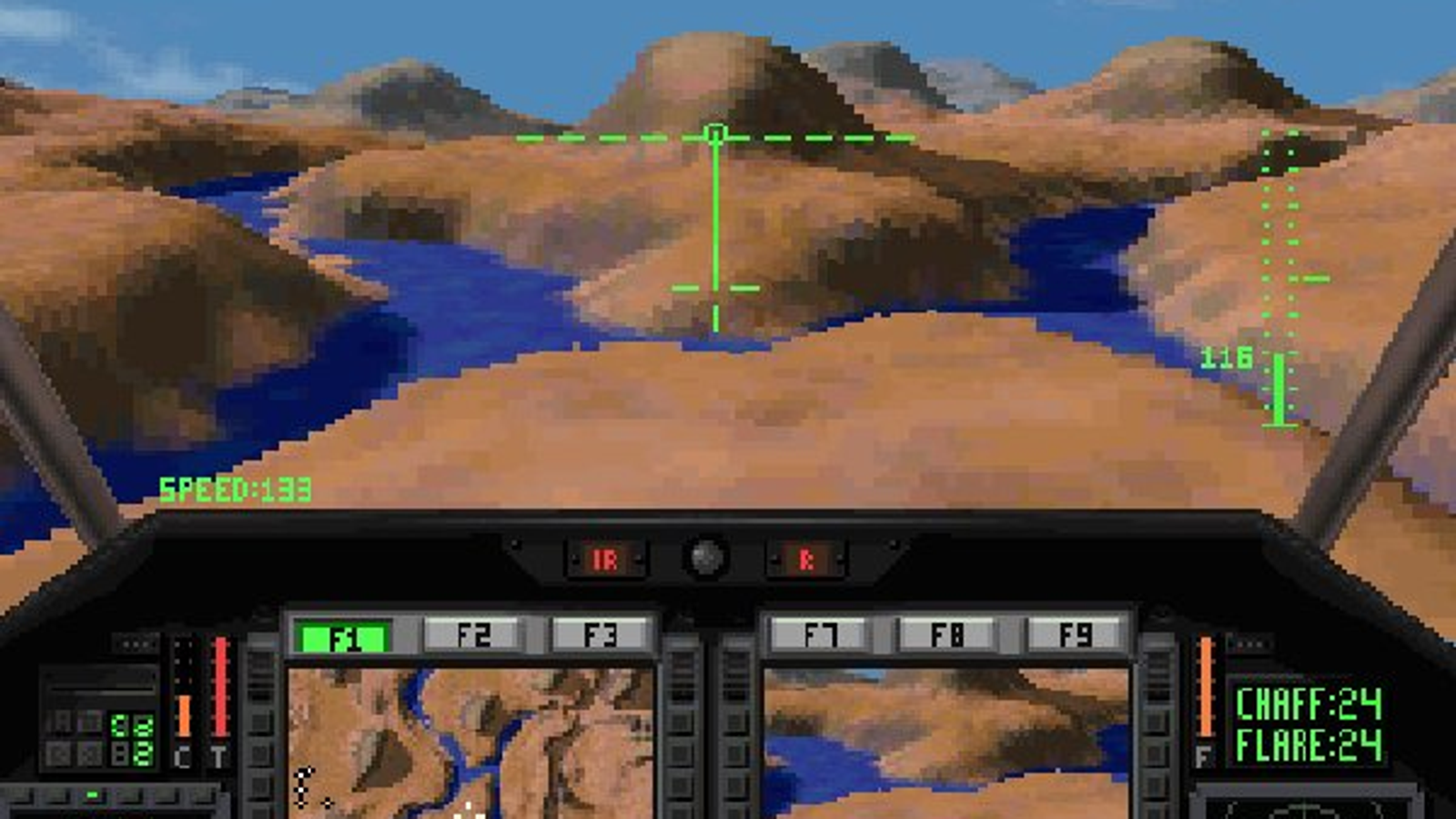
Image source: Rock Paper Shotgun - Voxel Pop's New Comanche Campaigns